Ampere Microarchitecture
This part dives into the SM architecture to reveal how execution units compete for resources. We'll examine how the A100's streaming multiprocessor (SM) architecture directly impacts instruction scheduling, particularly for INT and FP pipelines.
Each A100 SM contains 4 identical sub-cores that can execute instructions independently:
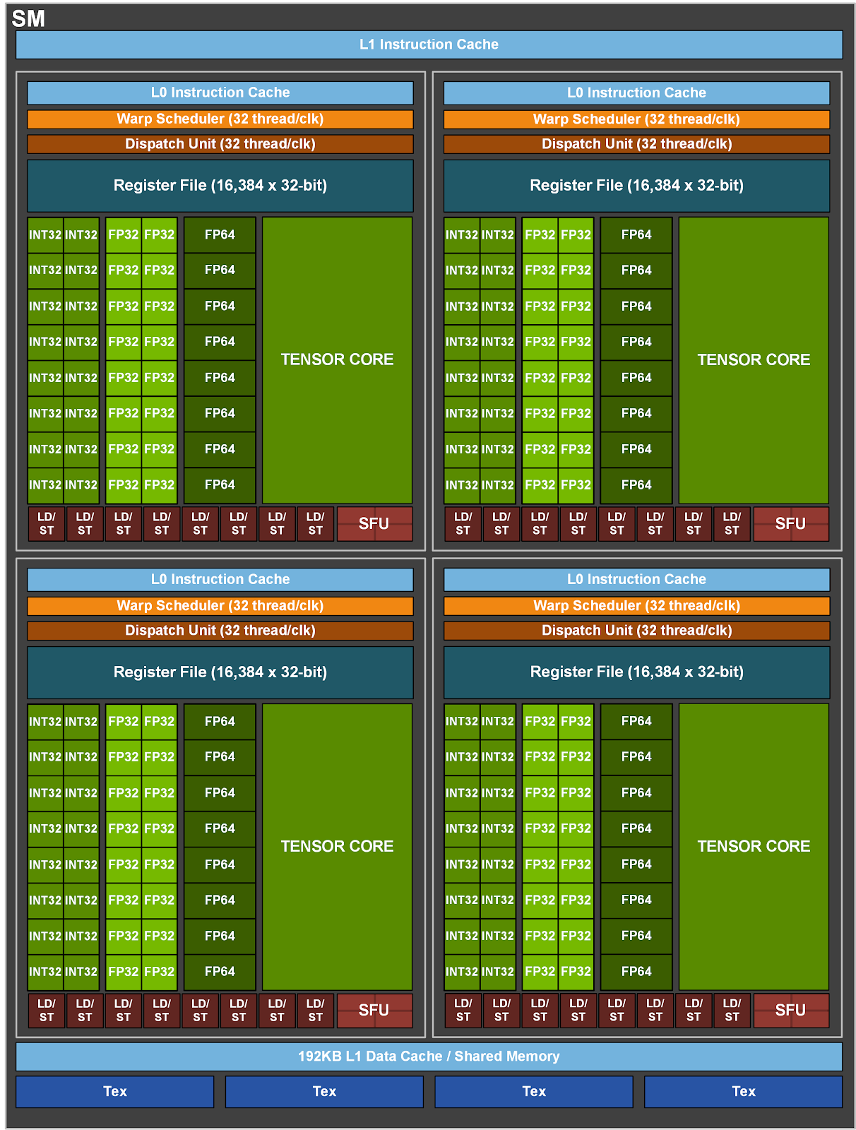
Let's zoom in on a single sub-core.
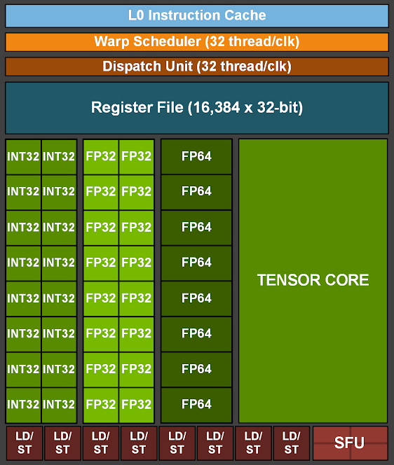
Looking at the sub-core architecture, we can see the execution units:
- 16x INT units: Handle logic operations and integer arithmetic (
MOV,LOP3,IADD3,SHF) - 16x FP32 units: Handle floating-point and integer multiplication (
FADD,FMUL,IMAD,IMUL). TheIMADinstruction can also emulate register copies (IMAD.MOV.U32), shifts (IMAD.SHL.U32), and additions (IMAD.IADD) - 4x SFUs: Special function units for complex operations (exponentials, trigonometry)
- There are much fewer SFU units than other circuits because they are expensive in terms of silicon
- As a result, they have much higher latency and lower throughput
- 1x Tensor Core: Executes matrix multiply-accumulate operations
Ampere Scalar Pipelines
Let's take a closer look at the FP32 and INT pipelines. Why does integer multiplication run on the FP32 pipeline? Because multiplication circuitry is complex and expensive in silicon area, and FP and INT multiplication share similar logic. Combining them saves die space.
Why emulate INT instructions on the FP32 pipeline instead of using the dedicated INT units? The answer lies in the dispatch constraints:
Throughput
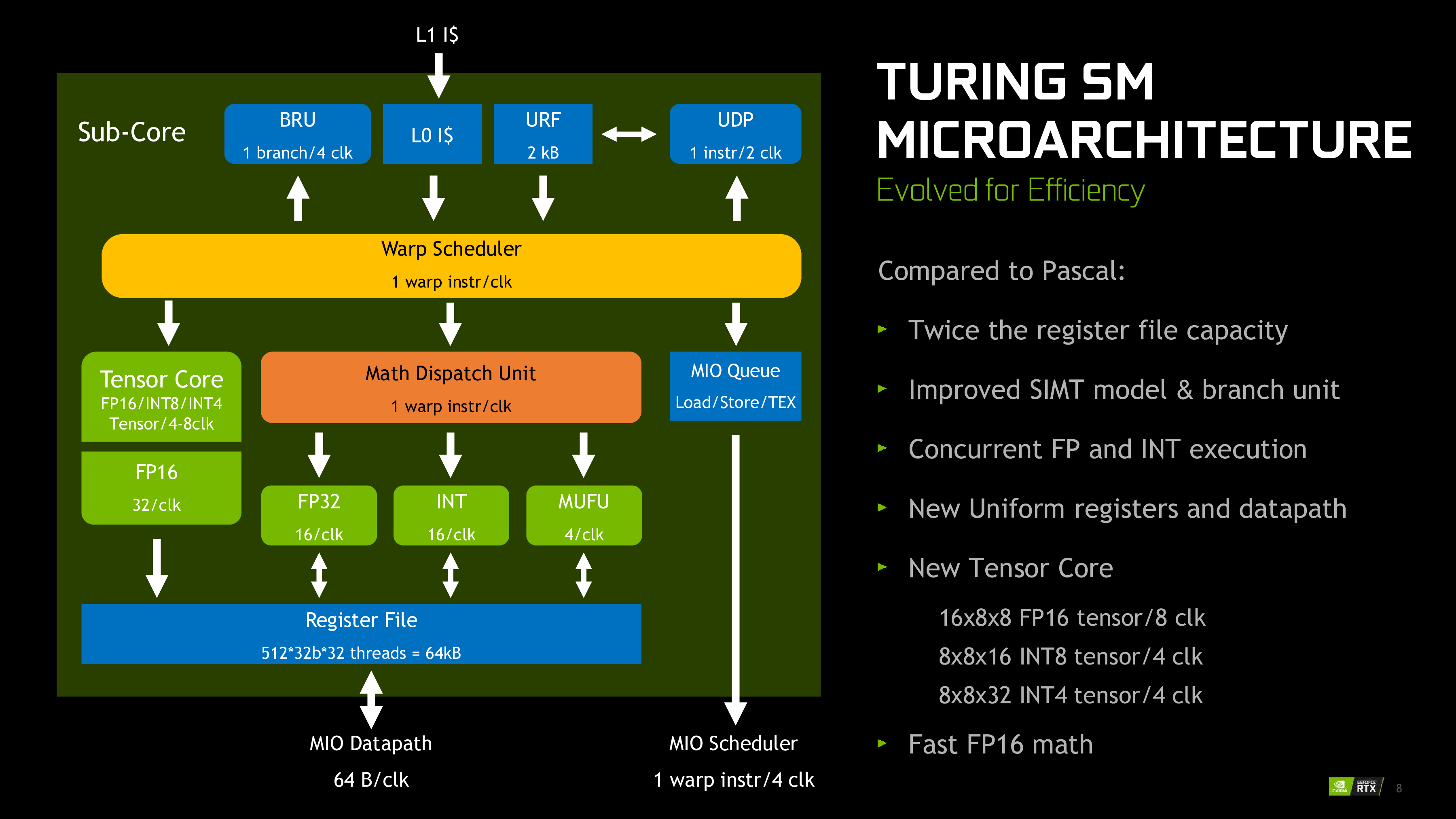
Even though this is a diagram of Turing, the numbers are accurate for the Ampere HPC, at least for the compute pipeline and warp scheduler.
- For FP32 & INT, we have 16 results per clock x 4 sub-cores = 64 results per SM/clock
- For MUFU, we have 4 results per clock x 4 sub-cores = 16 results per SM/clock, a much lower throughput
These align with the # results per clock per SM for CC 8.0 listed in this table.
Looking at this architecture, we can make several key observations:
First, only 1 instruction can be dispatched per clock per sub-core. Since each execution unit handles 16 operations per cycle but a warp contains 32 threads, any FP32 or INT instruction needs 2 cycles to complete execution (2 CPI). Importantly, this 2 CPI refers to the execution pipeline occupancy - not the dispatch scheduler.
This creates an opportunity for instruction interleaving. While an FP32 instruction occupies its execution pipeline for 2 cycles, the dispatch scheduler can issue a different instruction type on the very next cycle. For example:
- Cycle 0: Dispatch FP32 instruction (executes on FP32 pipeline, cycles 0-1)
- Cycle 1: Dispatch INT instruction (executes on INT pipeline, cycles 1-2)
Both instructions execute in parallel on their respective pipelines. This is why we can issue FP32 and INT instructions on back-to-back cycles despite each having 2 CPI - they use separate execution units.
This interleaving capability means certain integer operations (like shifts or register copies) can achieve higher effective throughput when mixed with FP32 operations. During FP-heavy blocks of instructions like softmax, we can schedule integer instructions in the gaps, utilizing cycles that would otherwise be wasted waiting for the FP32 pipeline to become available.
Interestingly, the INT pipeline also handles FP32 max/min operations (FMNMX) and FP32 to FP16 conversion (F2FP.PACK_AB). This explains why you might see these instructions interleaved with other FP32 instructions like FADD or FFMA.
Interleaving Beyond FP32 and INT
The interleaving pattern isn't limited to just FP32 and INT instructions. Instructions from any execution unit (like
ldmatrixfrom the LDST unit) can be issued back-to-back in consecutive cycles without stalling, provided that enough cycles have elapsed since the previous instruction from that unit (i.e., the instruction's CPI requirement is satisfied).
Microarchitecture Comparison
Comparing A100 and RTX 3090 SMs
| A100 | RTX 3090 |
|---|---|
| 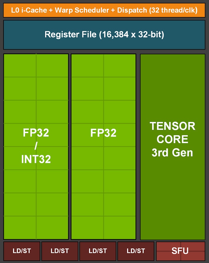 |
Let's compare the sub-core microarchitecture for the A100 and RTX 3090. Instead of 16x dedicated INT pipelines, the RTX 3090 has 16x hybrid pipelines that can handle either FP32 or INT operations. This means we can have either 32x FP32 or 16x INT results per clock.
This explains the increased FP32 throughput for SM 8.6 documented in the CUDA arithmetic instructions throughput table, where SM 8.6 doubles per-SM FP32 throughput vs 8.0 while maintaining the same INT throughput. Combined with clock speed and SM counts, this accounts for the roughly 50% lower FP32 throughput of the A100 vs 3090.
Device Throughput Revisited
In Why the A100 Suffers Throughput Ratios, we established that the A100 has a 16x mma:FP32 throughput ratio while the RTX 3090 has a 2x ratio. To get a deeper understanding, we'll verify these numbers at a low level by deriving them from instruction-level throughput.
For context, at the warp level:
- A single
mma.m16n8k16instruction executes 4096 FLOPs- the A100 can issue at 8 CPI (clocks per instr)
- the RTX 3090 can issue at 32 CPI (Sun et. al)
- A single FP32 FMA instruction executes 32×2 = 64 FLOPs
- the A100 issue rate is 2 CPI
- the RTX 3090 issue rate is 1 CPI
| Metric | A100 | RTX 3090 |
|---|---|---|
mma issue rate (clocks) | 8 | 32 |
| FP32 FMA issue rate (clocks) | 2 | 1 |
mma FLOPs/clock | 4096/8 = 512 | 4096/32 = 128 |
| FP32 FMA FLOPs/clock | 32 | 64 |
mma / FP32 FLOPs ratio | 512/32 = 16x | 128/64 = 2x |
Instruction Budget Analysis
This leads to an interesting exercise: how many instructions can we "afford" between tensor ops? To answer this, let's consider an ideal workload with no data dependencies - a best-case scenario for instruction scheduling.
A100: Between each pair of mma instructions (8 cycles each), we can fit:
- Up to 4 INT/FP32 instructions (non-interleaved)
- Up to 7 instructions (interleaved FP32+INT)
Here's an example of such a sequence:
mma
FP32
INT
FP32
INT
FP32
INT
FP32
mma
...
RTX 3090: With mma at 32 cycles, the budget is much larger:
- Up to 31 FP32 or 15 INT instructions (non-interleaved)
- Up to 31 instructions (interleaved)